NEWS


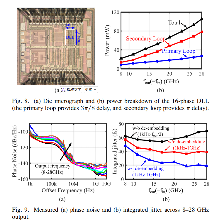
The research team presents a 16-phase delay-locked loop (DLL) operating from 8 to 28 GHz in 28-nm CMOS, targeting high-frequency multi-phase clock generation for wireline and mm-wave phased-array systems. To overcome the fundamental speed limitation imposed by the minimum inverter delay in conventional DLLs, a two-stage nested-feedback architecture is proposed.In the proposed design, the primary loop first generates clock phases with a spacing of 3π/8. Two secondary 8-phase DLLs further divide the phase domain to construct a complete 16-phase output set. Through carefully designed cross-coupled feedback between the two stages, the primary and secondary loops remain orthogonal, ensuring that delay variations in one loop do not propagate to the other. This significantly improves PVT robustness and reduces phase error accumulation.To address systematic phase distortion caused by duty-cycle imbalance in multi-stage delay cells, an AC-coupled delay-unit structure is introduced. By balancing pull-up and pull-down currents, the proposed technique effectively suppresses duty-cycle variation accumulation and improves phase accuracy.
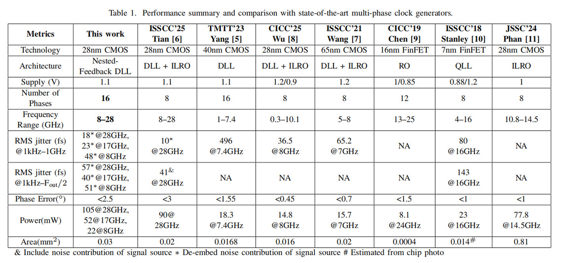
Fabricated in 28-nm CMOS technology, the prototype achieves stable operation across 8–28 GHz, with measured integrated jitter below 47 fs and 3σ phase error less than 2.5°. The proposed architecture relaxes the critical path delay by more than 50% compared to conventional DLLs while maintaining closed-loop operation.This work provides a compact and robust solution for low-jitter multi-phase clock generation in high-speed wireline transceivers and mm-wave phased-array systems.
This work was published in IEEE Radio Frequency Integrated Circuits Symposium (RFIC) in 2026, with Junyan Bi as first author. He is currently pursuing the Ph.D. degree in integrated circuit science and engineering with Fudan University, Shanghai.
Paper:J. Bi, et.al, An 8–28-GHz 16-Phase Delay Locked Loop Employing Nested Feedback Loops in 28-nm CMOS, in 2026 IEEE Radio Frequency Integrated Circuits Symposium.